Product Short Description
Product Overview
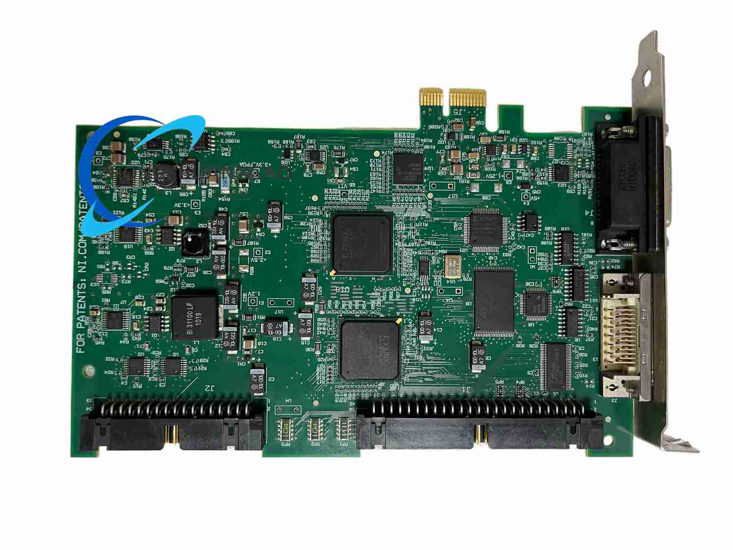
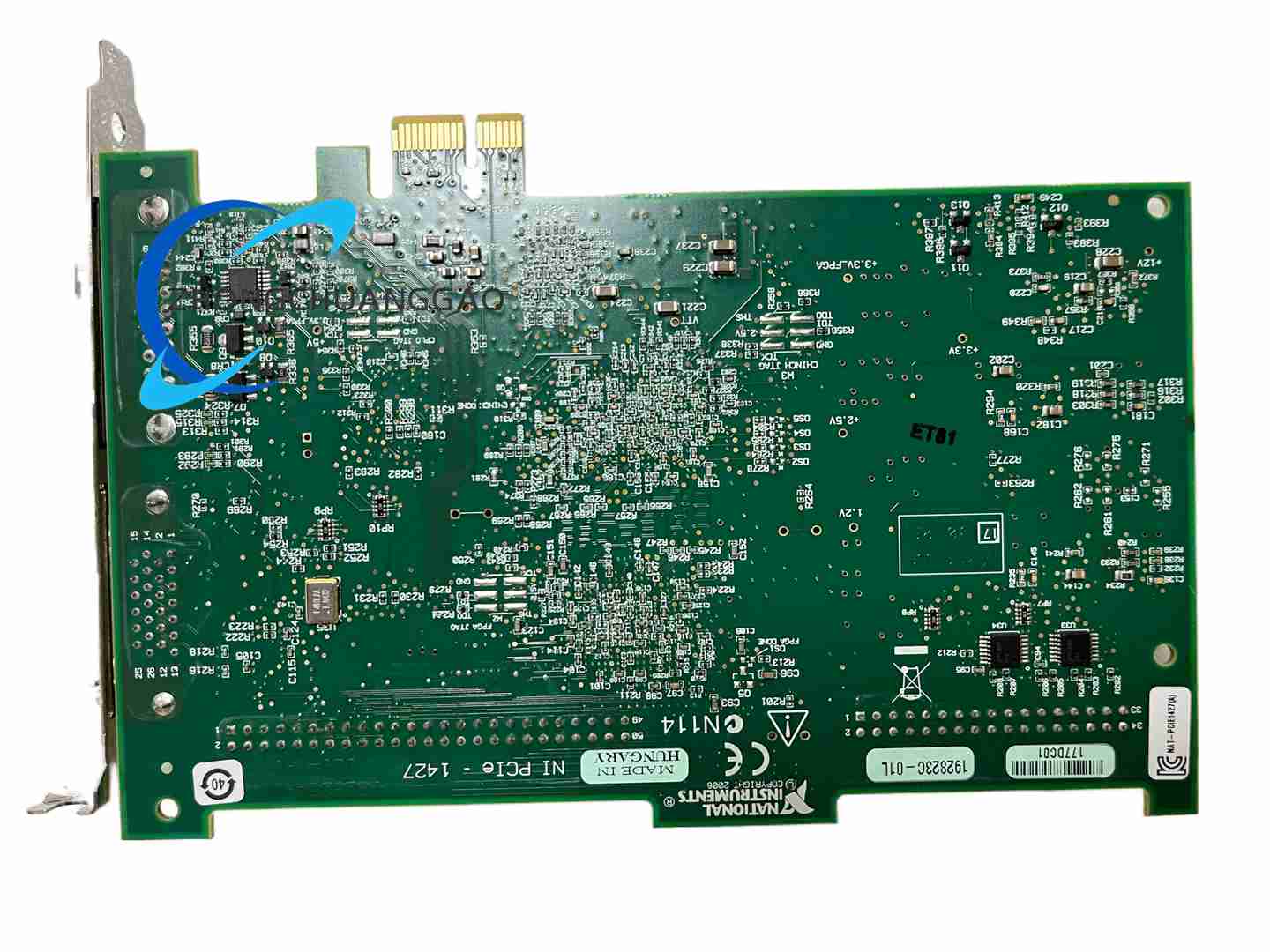
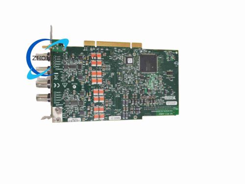
The PCIE-1427 is a high-performance PCI Express bus Camera Link image acquisition hardware developed by National Instruments, specially designed for industrial machine vision high-speed digital camera image data collection. This device supports full standard Camera Link industrial digital camera communication protocol, integrates high-bandwidth PCI Express x4 bus interface and large-capacity onboard image cache memory, applied to high-speed product defect detection, high-precision visual measurement, semiconductor wafer inspection, medical digital imaging high-speed image acquisition scenarios.
Description
Camera Link Interface
- Supported Camera Link Modes: Base, Medium, Full standard Camera Link transmission modes
- Maximum Image Data Bandwidth: 6.8 Gbit/s peak image data receiving bandwidth
- Supported Camera Bit Depth: 8-bit, 10-bit, 12-bit, 14-bit, 16-bit monochrome and color pixel data
- Camera Control Signal Channels: Bidirectional serial communication channel for camera parameter configuration; programmable digital trigger input and output lines for camera exposure synchronization and external test fixture trigger
PCI Express Bus Interface
- Bus Standard: PCI Express x4 Gen 1 bus
- Maximum Bus Transmission Bandwidth: 1 GB/s bidirectional image data transmission bandwidth
- DMA Data Transmission Mode: Hardware direct memory access transmission without CPU occupation
Onboard Image Cache Memory
- Dedicated Onboard Image Buffer Capacity: 256 MB high-speed DDR2 cache memory
- Cache Working Modes: Circular buffer continuous image storage, multi-frame snapshot buffer storage, real-time streaming image transmission
Timing & Synchronization System
- Onboard high-precision trigger clock generator
- Internal Reference Clock Accuracy: ±25 ppm under 25 ℃ standard working temperature
- Multi-board Synchronization: NI-IMAQ Trigger Bus hardware interface supports multi-image acquisition board synchronous camera triggering and image data collection
9.4 Functional Features
- Full Camera Link Base/Medium/Full three standard mode compatibility, supporting all mainstream industrial monochrome and color Camera Link digital high-speed cameras on the market
- 6.8 Gbit/s ultra-high image data receiving bandwidth, realizing continuous high frame rate large resolution image collection without frame loss
- 256 MB large-capacity onboard DDR2 image cache memory, storing multi-frame image data to avoid image frame loss caused by temporary host computer memory bandwidth bottleneck
- PCI Express x4 Gen1 high-speed DMA transmission mode, directly transmit image data from onboard cache to host computer system memory without occupying CPU computing resources, guaranteeing real-time image data transmission performance
- Bidirectional serial communication channel for real-time configuration of internal parameters of connected Camera Link cameras, including exposure time, gain, white balance, trigger mode and other camera control parameters
- Programmable digital trigger input and output lines, realizing synchronous exposure triggering of multiple cameras, and output trigger signals to synchronize external industrial conveyor belts, lighting controllers and automatic test fixtures
- Complete NI-IMAQdx and NI-IMAQ vision driver compatibility, supporting LabVIEW Vision Development Module, Python OpenCV, C# C++ mainstream machine vision development environments
- Multi-board synchronous triggering function through NI-IMAQ Trigger Bus, realizing multi-camera synchronous image acquisition for 3D visual measurement, multi-angle product defect detection large-scale machine vision systems
9.5 Application Scenarios
- Electronic assembly line PCB surface high-speed defect visual inspection
- Semiconductor wafer chip surface microscopic defect high frame rate image capture
- Automobile parts dimensional high-precision visual measurement and surface scratch detection
- Medical digital radiography high-speed digital image data acquisition
- Packaging industry product appearance defect real-time visual detection on high-speed conveyor belts
- Aerospace component high-precision 3D visual scanning multi-camera synchronous image collection
- Laboratory high-speed microscopic imaging equipment continuous image recording
9.6 Performance Parameters (Typical under 25℃)
- Continuous Operating Temperature Range: 0 ℃ ~ 55 ℃
- Storage Temperature Range: -40 ℃ ~ 85 ℃
- Peak Total Power Consumption: 23.5 W
- Maximum Continuous Uninterrupted Working Time: 720 hours without image data transmission bandwidth attenuation
- Maximum Supported Camera Resolution & Frame Rate: 4K resolution 120 frames per second continuous image acquisition under Camera Link Full mode
9.7 Material & Construction Composition
- Main Circuit Substrate: Multi-layer FR-4 high-speed low-loss printed circuit board, independent Camera Link high-speed signal transmission layer, PCI Express bus communication layer and DDR2 cache memory power supply ground plane, controlled impedance high-speed signal traces layout
- Core Processing Chips: High-speed Camera Link data receiving interface chip, Xilinx high-performance FPGA image data processing and timing control chip, 256 MB DDR2 high-speed cache memory chip, PCI Express x4 bus communication interface chip
- Front Panel Connector: High-shielding metal Camera Link MDR multi-pin connector with built-in EMI rubber sealing gasket for camera data cable connection; additional multi-pin shielded D-SUB connector for digital trigger input and output wiring
- Mechanical Fixing Components: Cold rolled steel full-height PCI Express mounting bracket with zinc anti-corrosion electroplating surface treatment
- Passive High-speed Components: Low-inductance thin-film precision matching resistors for controlled impedance traces, low-loss high-frequency ceramic bypass capacitors, high-frequency ferrite EMI suppression beads for all Camera Link high-speed signal traces
9.8 Structural Characteristics
- Form Factor: Standard full-height PCI Express x4 Gen1 expansion board
- Physical Overall Dimensions: Width 10.6 cm, Length 17.5 cm
- PCB High-speed Signal Isolation Design: Camera Link high-speed differential signal transmission area and PCI Express bus digital communication area separated by continuous copper ground guard ring to eliminate high-frequency signal crosstalk
- Controlled Impedance High-speed Traces Layout: All Camera Link differential image signal PCB traces manufactured to precise 100 Ω differential controlled impedance specifications to prevent high-speed digital signal reflection and data transmission error
- Thermal Dissipation Layout: High-density copper thermal vias laid under FPGA high-speed processing chip and DDR2 cache memory chip for passive convection heat dissipation without additional cooling fans
- EMI/RF Shielding Layout: Closed copper ground shielding layer around all Camera Link high-speed differential signal traces to block external industrial high-frequency electromagnetic interference signal coupling and avoid image data transmission bit error
9.9 Working Principle
- Camera Link High-speed Image Data Receiving Stage: Connected industrial Camera Link digital camera transmits pixel image data and camera synchronous clock signal to PCIE-1427 via Camera Link differential shielded cable; high-speed Camera Link receiving interface chip converts differential high-speed digital signal into single-ended digital data stream and transmits to onboard FPGA processing chip
- FPGA Image Data Processing & Cache Control Logic: Onboard high-performance FPGA receives continuous image pixel data stream sent by Camera Link interface chip; FPGA temporarily stores received image frame data into 256 MB onboard DDR2 high-speed circular cache memory according to user-configured cache mode; FPGA generates precise synchronous trigger clock signals for camera exposure control and external test fixture synchronization; FPGA completes serial communication data parsing and transmission to realize camera internal parameter real-time configuration
- PCI Express DMA High-speed Data Transmission Stage: When host computer vision application software sends image data reading instructions, onboard FPGA controls DMA hardware transmission module to directly read complete image frame data from DDR2 cache memory; DMA module transmits image data to host computer system memory through PCI Express x4 Gen1 high-speed bus without occupying CPU core computing resources, guaranteeing real-time continuous image data streaming transmission performance
- Multi-board Synchronization Trigger Logic: NI-IMAQ Trigger Bus transmits unified high-precision synchronous trigger clock signals between multiple PCIE-1427 image acquisition boards; all connected image acquisition boards receive the same synchronous trigger signal at the same time, realizing perfectly synchronized multi-camera image frame exposure and data collection for large-scale multi-angle machine vision measurement systems
9.10 Installation Requirements
- Host PC Expansion Slot: Unoccupied full-height PCI Express x4 Gen1 motherboard expansion slot; computer chassis must be equipped with forced air cooling fan to maintain internal temperature within rated operating range during continuous high-speed image data collection
- Pre-operation Warm-up Requirement: After powering on the host computer, maintain continuous power supply for at least 12 minutes before executing high frame rate high-resolution image acquisition tasks to stabilize high-speed differential signal transmission performance and eliminate thermal drift induced image data bit error
- Mechanical Installation Steps: Remove the metal blank baffle of the chassis PCI Express expansion slot; align the gold-plated edge connector of the PCIE-1427 board with the motherboard PCI Express x4 slot; fully insert the board until the connector is completely seated; tighten the fixing screw of the steel mounting bracket to the chassis frame to eliminate PCB mechanical vibration during high-speed data transmission
- High-speed Camera Link Cable Wiring Specifications: Use standard fully shielded Camera Link MDR high-speed differential cables matching the camera transmission mode; minimize cable length to reduce high-frequency signal attenuation and bit error rate; connect the outer metal shielding layer of the Camera Link cable to the metal shell of the board front panel MDR connector to form low-impedance EMI ground reference; strictly separate Camera Link high-speed image signal cables from high-current power, motor drive and digital control cables by a minimum distance of 20 cm to avoid high-frequency electromagnetic interference induced image data transmission error
- Software Driver Installation Process: Download and install the latest NI-IMAQdx vision driver software matching the host operating system; launch NI MAX hardware configuration tool, the software automatically identifies PCIE-1427 image acquisition hardware equipment; configure Camera Link transmission mode, image cache storage mode, camera serial communication parameters and digital trigger signal parameters in NI MAX software according to connected industrial camera model and machine vision test system requirements
9.11 Operation Precautions
- Camera Link Cable Impedance Matching Restriction: Only use standard 100 Ω differential impedance fully shielded Camera Link MDR cables; mismatched cable impedance will cause high-speed digital signal reflection, severe image data bit error and complete image frame loss
- ESD Static Discharge Protection Rule: Wear a grounded anti-static wristband before touching PCB boards, MDR/D-SUB connectors and internal high-speed FPGA, DDR2 memory circuit components; electrostatic discharge will permanently damage sensitive high-speed digital signal processing chips and cause irreversible image data transmission failure
- Chassis Cooling Mandatory Requirement: Do not run PCIE-1427 with the side panel of the host computer chassis removed during continuous high frame rate image acquisition operation; insufficient air convection will cause serious thermal drift of high-speed differential signal transmission circuit, increased image data bit error rate, reduced maximum supported camera frame rate and distorted captured image frames
- Cable Separation Specification: Strictly separate Camera Link high-speed image signal cables and high-power industrial wiring, inverter drive cables to prevent high-frequency electromagnetic interference from introducing data bit error into image transmission signals
- Calibration Cycle Regulation: Execute onboard high-speed signal timing self-calibration every 30 days of continuous high-speed image acquisition operation; complete full external factory calibration with NI certified Camera Link reference signal equipment once per calendar year
Reviews
There are no reviews yet.