
Product Short Description
Product Overview
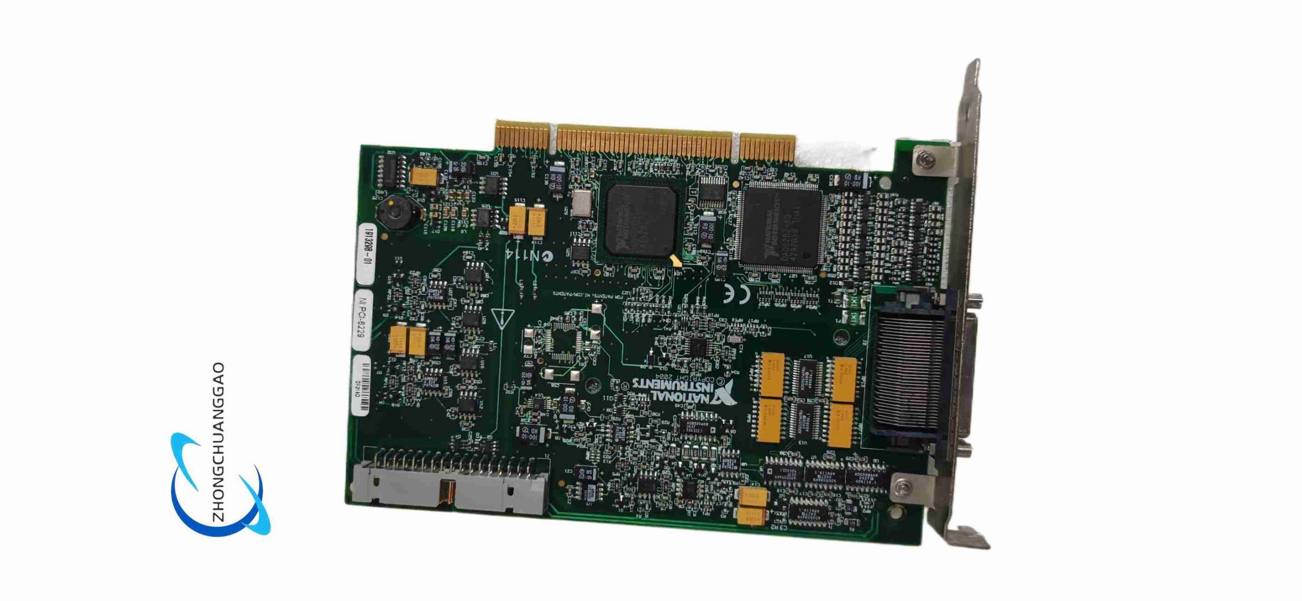
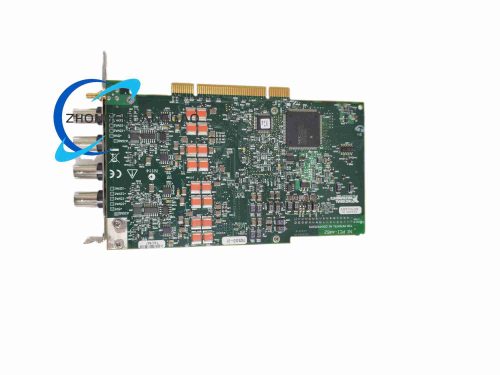
The PCI-6229 belongs to NI M Series medium-speed multifunction DAQ hardware, designed for industrial automation, laboratory measurement and medium-speed mixed signal test applications. This PCI bus integrated device combines multi-channel analog input, analog output, bidirectional digital I/O and high-resolution counter timer modules, balancing channel quantity, sampling speed and cost performance for mainstream measurement control demands.
Description
Analog Input
- Channel Configuration: 32 single-ended input channels or 16 true differential input channels, software dynamic switching
- ADC Resolution: 16-bit successive approximation analog-to-digital converter
- Maximum Single-channel Sampling Rate: 250 kS/s
- Programmable Input Voltage Ranges: ±0.1 V, ±0.2 V, ±1 V, ±2 V, ±5 V, ±10 V
- Input Bandwidth: 1.5 MHz full power bandwidth per channel
- Common Mode Rejection Ratio: >100 dB at 50 Hz industrial interference frequency
Analog Output
- Channel Count: 4 independent single-ended analog output channels
- DAC Resolution: 16-bit digital-to-analog converter
- Maximum Update Rate: 833 kS/s total aggregate output sampling rate
- Fixed Output Voltage Range: ±10 V
- Built-in full short-circuit protection with automatic current limiting circuit
Digital I/O Interface
- Total Digital Channels: 48 bidirectional TTL digital I/O lines divided into six independent 8-bit ports
- Logic Standard: 5 V TTL compatible, high-level threshold 2.0 V, low-level threshold 0.8 V
- Single Channel Drive Capacity: Maximum 2.4 mA sink and source current
- Programmable digital input filter for suppressing industrial contact bounce noise
Counter & Timer Subsystem
- Counter Quantity: Two independent 32-bit high-resolution event counters
- Maximum Counter Input Frequency: 80 MHz
- Supported Working Modes: Edge counting, frequency measurement, pulse width capture, quadrature encoder position tracking, PWM pulse signal generation
Timing Synchronization System
- Internal Reference Clock Accuracy: ±50 ppm under 25 ℃ standard working temperature
- Multi-board Synchronization: RTSI bus hardware interface supports synchronous clock and trigger signal transmission among multiple M Series DAQ boards
6.4 Functional Features
- Flexible dual input mode switching, supporting high-density single-ended multi-channel measurement and low-noise differential signal collection for weak sensors
- 32-bit ultra-long counter architecture, eliminating frequent counter overflow interrupts during long-time continuous pulse acquisition
- Four-channel analog output design realizes multi-variable closed-loop control for multi-actuator industrial equipment
- 48-channel mass digital I/O ports meet large-scale relay matrix control, multi-point limit switch detection and parallel digital communication requirements
- Onboard programmable digital filter suppresses mechanical switch bounce and industrial electromagnetic interference noise on digital input signals
- Independent per-channel analog input gain configuration allows mixed deployment of thermocouples, strain gauges, voltage transmitters in one test system
- Complete NI-DAQmx driver compatibility, supporting LabVIEW, Python, MATLAB, C#, C++ mainstream development environments
- Built-in automatic self-calibration function, real-time correcting gain drift and offset error caused by ambient temperature changes
6.5 Application Scenarios
- Industrial assembly line multi-point temperature, pressure, flow sensor real-time monitoring
- Closed-loop multi-axis motion control system analog feedback signal acquisition and analog actuator drive
- Material tensile, compression mechanical performance laboratory multi-sensor synchronous testing
- Battery pack charge-discharge cycle voltage current multi-channel synchronous measurement
- Automatic test equipment for low-speed analog electronic circuit verification
- University mechanical, electrical engineering laboratory general data acquisition teaching platform
- Building environmental monitoring multi-channel temperature and humidity transmitter signal collection
6.6 Performance Parameters (Typical under 25℃)
- Continuous Operating Temperature Range: 0 ℃ ~ 55 ℃
- Storage Temperature Range: -40 ℃ ~ 85 ℃
- Peak Total Power Consumption: 17.6 W
- Minimum Warm-up Time to Reach Full Rated Accuracy: 10 minutes continuous power supply
- Maximum Continuous Uninterrupted Working Time: 720 hours without accuracy attenuation
6.7 Material & Construction Composition
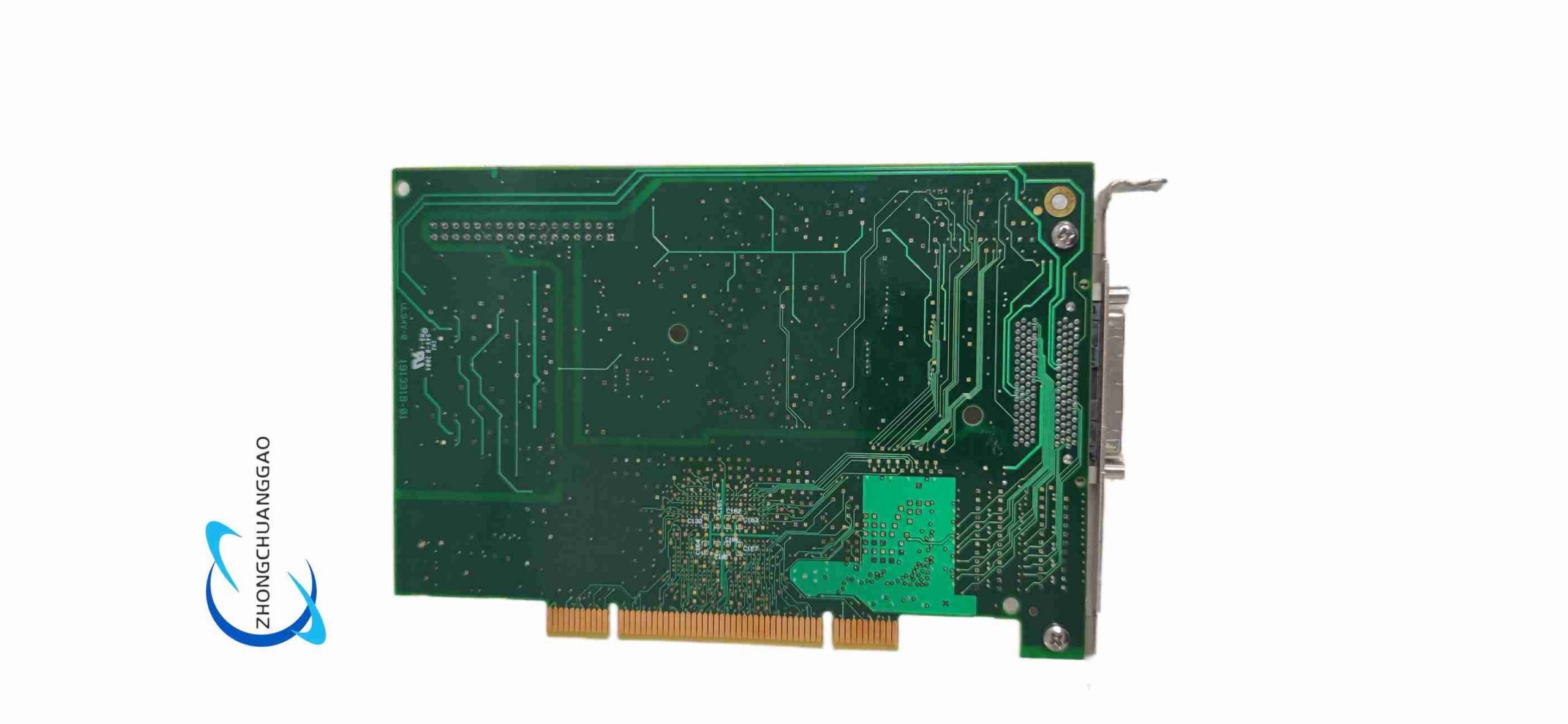
- Main Circuit Substrate: Multi-layer FR-4 fire-resistant printed circuit board, independent analog ground, digital ground and power supply ground three-layer separated ground plane to isolate digital switching noise
- Core Processing Chips: 16-bit multi-channel successive approximation ADC, four-channel 16-bit DAC, low-noise JFET input operational amplifiers, Xilinx dedicated timing control FPGA, dual 32-bit counter logic integrated circuits
- Front Panel Connector: Multi-pin metal shielded D-SUB connector with built-in EMI rubber sealing gasket for all analog, digital and counter wiring terminals
- Mechanical Fixing Components: Cold rolled steel full-height PCI mounting bracket with zinc anti-corrosion electroplating surface treatment
- Passive Electronic Components: Low temperature drift metal film precision resistors, low noise polypropylene signal capacitors, ferrite magnetic bead EMI suppression components for all input and output signal traces
6.8 Structural Characteristics
- Form Factor: Standard full-length 32-bit 33 MHz PCI bus expansion board
- Physical Overall Dimensions: Width 10.6 cm, Length 17.5 cm
- PCB Regional Isolation Design: Analog front-end circuit area and digital FPGA, counter logic area separated by continuous copper ground guard ring to avoid signal crosstalk
- Thermal Dissipation Layout: High-density copper thermal vias laid under FPGA, ADC and DAC high-power chips for passive convection heat dissipation without additional cooling fans
- EMI Shielding Layout: Closed copper ground shielding layer around all analog signal traces to block external industrial electromagnetic interference signal coupling
6.9 Working Principle
- Analog Input Signal Conditioning Stage: External sensor analog voltage signal enters per-channel independent buffer amplifier; software controlled programmable gain circuit amplifies weak sensor signals to match ADC full-scale range; single-ended/differential multiplexer switches signal transmission path according to user configuration
- 16-bit Successive Approximation ADC Conversion: Multiplexed analog voltage signal is sampled and held; successive approximation ADC completes binary search analog-to-digital conversion and outputs 16-bit binary digital data; converted data is temporarily stored in onboard FIFO buffer memory
- FPGA Timing and Digital I/O Control Logic: Onboard dedicated FPGA generates programmable sample clock and trigger signals for analog input and output channels; FPGA completes digital port direction switching, digital input filter noise suppression and digital signal transmission control to PCI bus
- 32-bit Counter Timer Operation: External pulse, quadrature encoder signals enter counter input buffer circuits; 32-bit counter logic accumulates pulse counts, measures input signal frequency and pulse width, and outputs variable frequency digital pulse signals synchronized with board master clock
- Four-channel Analog Output DAC Conversion: Host computer transmits target analog voltage digital data to onboard DAC FIFO memory; each independent 16-bit DAC converts discrete digital sample values into continuous analog voltage signals to drive external actuators and test fixtures
- RTSI Multi-board Synchronization Logic: RTSI bus transmits unified master clock and trigger signals between multiple PCI-6229 boards, realizing fully synchronous multi-card multi-channel analog signal collection and analog waveform output
6.10 Installation Requirements
- Host PC Expansion Slot: Unoccupied full-length 32-bit PCI motherboard expansion slot; computer chassis must be equipped with forced air cooling fan to maintain internal temperature within rated operating range
- Pre-operation Warm-up Requirement: After powering on the host computer, maintain continuous power supply for at least 10 minutes before executing high-precision DC voltage measurement tasks to eliminate thermal drift errors
- Mechanical Installation Steps: Remove the metal blank baffle of the chassis expansion slot; align the gold-plated edge connector of the PCI board with the motherboard PCI slot; fully insert the board until the connector is completely seated; tighten the fixing screw of the steel mounting bracket to the chassis frame to eliminate PCB mechanical vibration
- Signal Wiring Specifications: All analog sensor signal wiring adopts double shielded twisted pair cables; connect the outer shielding layer of the cable to the metal shell of the D-SUB connector to form low-impedance EMI ground reference; separate analog signal cables from high-current power cables and motor drive cables by a minimum distance of 10 cm to avoid electromagnetic interference
- Software Driver Installation Process: Download and install the latest NI-DAQmx driver software matching the host operating system; launch NI MAX hardware configuration tool, the software automatically identifies PCI-6229 hardware equipment; execute onboard self-calibration program after hardware identification to correct channel gain and offset errors
6.11 Operation Precautions
- Analog Input Overvoltage Restriction: Do not input analog voltage exceeding ±10 V peak value; excessive voltage will permanently damage front-end buffer amplifier circuits
- ESD Static Discharge Protection Rule: Wear a grounded anti-static wristband before touching PCB boards, connectors and internal circuit components; electrostatic discharge will permanently damage sensitive ADC, DAC and FPGA chips
- Chassis Cooling Mandatory Requirement: Do not run PCI-6229 with the side panel of the host computer chassis removed; insufficient air convection will cause serious thermal drift, increased measurement noise and inaccurate voltage reading data
- Cable Separation Specification: Strictly separate low-level analog sensor cables and high-power industrial wiring to prevent electromagnetic interference from introducing noise into measurement signals
- Calibration Cycle Regulation: Execute onboard self-calibration every 45 days of continuous operation; complete full external factory calibration with NI certified reference voltage equipment once per calendar year
- Storage Environment Requirements: When uninstalled from the host computer, store PCI-6229 in the original factory anti-static packaging bag; avoid long-term storage in high humidity, dusty and extreme temperature environments
- Digital I/O Current Limit Warning: Do not make single digital channel sink or source current exceed 2.4 mA; excessive current will burn out digital output driver circuits permanently
Reviews
There are no reviews yet.