
Product Short Description
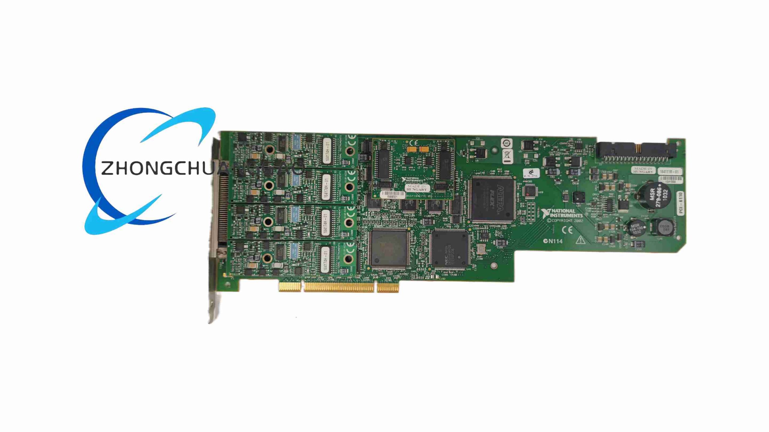
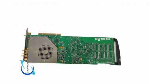
The PCI-6110 is a high-speed simultaneous sampling multifunction PCI DAQ board designed for high-bandwidth transient signal measurement applications requiring fully synchronized multi-channel analog input capture. It features four independent simultaneously sampled analog input channels with 5 MS/s per-channel maximum sampling rate, paired with dual analog output channels, 8 bidirectional digital I/O lines and dual 24-bit counter/timer modules for mixed-signal test and measurement systemsNI
Description
Simultaneous Analog Input (AI)
- Channel Count: 4 fully independent true differential simultaneously sampled input channels
- ADC Resolution: 12-bit high-speed successive approximation converter
- Maximum Per-Channel Sampling Rate: 5 MS/s synchronous sampling across all four input channels
- Input Voltage Ranges: Software-selectable ±0.2 V, ±1 V, ±5 V, ±10 V
- Input Bandwidth: 2 MHz full-power bandwidth per channel
- Inter-Channel Skew: < 10 ns between all four simultaneous input channels
Analog Output (AO)
- Channel Count: 2 single-ended analog output channels
- DAC Resolution: 12-bit digital-to-analog converter
- Maximum Per-Channel Update Rate: 1 MS/s
- Output Voltage Range: ±10 V
- Short-Circuit Protection: Automatic current limiting for indefinite output short-circuit tolerance
Digital I/O (DIO)
- Channel Count: 8 bidirectional TTL-compatible digital I/O lines
- Logic Level: 0–5 V TTL, 2.0 V logic high threshold, 0.8 V logic low threshold
- Maximum Sink/Source Current per Channel: 4 mA
Counter/Timer Subsystem
- Independent Counter Channels: 2 × 24-bit event counters
- Counter Clock Input Frequency Range: DC to 25 MHz
- Supported Counter Modes: Event counting, frequency measurement, pulse width capture, quadrature encoder position tracking, variable-frequency pulse generation
Timing & Synchronization
- Internal Timebase Accuracy: ±25 ppm at 25 °C
- Multi-Board Synchronization: RTSI bus interface for shared high-speed clock and trigger signals across multiple PCI-6110 DAQ boards
5.4 Functional Features
- Four fully synchronous true differential analog input channels with <10 ns inter-channel skew for precise transient multi-point signal capture without phase offset between measurement channels
- High-speed 5 MS/s per-channel simultaneous sampling capability for high-bandwidth transient signal measurement including shock, vibration, ultrasonic and pulsed electrical signals
- 12-bit high-speed successive approximation ADC architecture optimized for ultra-fast sampling and transient signal capture
- Dual 12-bit analog output channels for high-speed arbitrary waveform stimulus generation for transient test fixture excitation
- 8-channel bidirectional TTL digital I/O for digital control of test relays, limit switch input monitoring and synchronization with external digital test equipment
- Dual independent 24-bit high-frequency counter/timer modules for high-speed pulse counting, rotational speed measurement and quadrature encoder position tracking for motion control test systems
- RTSI bus high-speed multi-board synchronization enabling scalable multi-card simultaneous sampling measurement systems with perfectly phase-aligned channel timing
- Full NI-DAQmx driver compatibility supporting LabVIEW, MATLAB, Python, C/C++ and Visual Studio development environments for custom transient test automation software development
5.5 Application Scenarios
- Automotive crash test transient shock and acceleration signal multi-channel synchronous measurement
- Ultrasonic non-destructive material inspection high-speed pulsed signal acquisition
- Power electronics inverter, motor drive and switching power supply transient voltage/current waveform capture
- Structural shock and impact testing for aerospace component durability validation
- Radar and sonar pulsed signal front-end analog waveform synchronous measurement
- High-speed motion control system quadrature encoder position tracking and pulse frequency measurement
- Electronic semiconductor mixed-signal IC transient production test and validation
5.6 Performance Parameters (Typical at 25°C)
- Operating Temperature Range: 0 °C to 55 °C
- Storage Temperature Range: -40 °C to 85 °C
- Peak Power Consumption: 19.4 W
- Minimum Warm-Up Time for Full Accuracy: 12 minutes continuous power operation
5.7 Material & Construction Composition
- Main Printed Circuit Board: Multi-layer FR-4 high-speed low-capacitance circuit board with fully separated analog, digital and power ground planes to minimize high-speed switching noise coupling to sensitive analog signal paths
- Core High-Speed Signal ICs: Four independent 12-bit high-speed successive approximation ADC chips (one dedicated per input channel), dual 12-bit DAC chips, low-distortion high-bandwidth JFET input operational amplifiers, high-performance FPGA high-speed timing and data processing controller, 24-bit high-frequency counter/timer logic ICs
- Front Panel Connector: Multi-channel shielded metal D-SUB connector with integrated EMI suppression gaskets for all analog, digital and counter I/O wiring connections
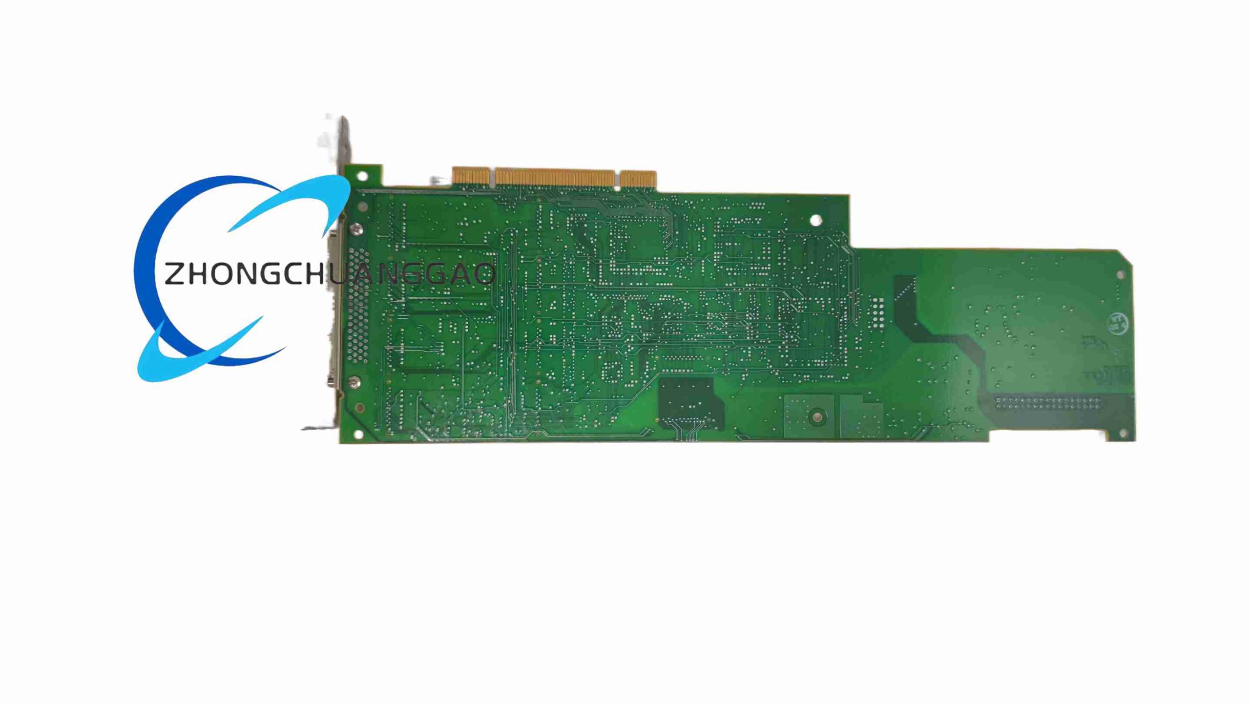
- Mechanical Mounting Hardware: Zinc-plated cold-rolled steel full-height PCI retention bracket
- Passive High-Speed Components: Low-inductance thin-film precision resistors, low-loss ceramic bypass capacitors, high-frequency ferrite EMI suppression beads on all analog signal PCB traces
5.8 Structural Characteristics
- Form Factor: Standard full-length 32-bit PCI 33 MHz bus compliant expansion board
- Physical Dimensions: 10.6 cm width × 17.5 cm length
- PCB High-Speed Zone Isolation: Strict physical partitioning of each individual analog input channel’s front-end circuitry via independent copper ground guard rings to eliminate inter-channel crosstalk during high-speed simultaneous sampling
- Controlled-Impedance High-Speed Traces: All analog input signal PCB traces manufactured to precise controlled impedance specifications to prevent high-speed signal reflection and waveform distortion
- Thermal Dissipation Design: Dense copper thermal vias under each dedicated ADC chip and high-power FPGA timing controller for passive convection heat dissipation during continuous high-speed sampling operation
- EMI/RF Shielding: Continuous full-perimeter copper ground shielding layer surrounding all analog signal traces to block external industrial high-frequency electromagnetic interference
5.9 Working Principle
- Per-Channel Independent Analog Input Conditioning Stage: Each of the four true differential input channels features dedicated isolated buffer and programmable gain amplifier circuitry; external transducer differential signal enters channel-specific conditioning circuit; software-selectable gain adjusts signal amplitude to match dedicated ADC full-scale input range
- Dedicated Per-Channel 12-Bit High-Speed ADC Conversion: Every analog input channel is paired with an independent high-speed successive approximation ADC chip; all four ADC chips receive identical synchronized sample clock signals from onboard FPGA timing controller, enabling perfectly simultaneous analog-to-digital conversion across all four input channels with minimal inter-channel timing skew
- High-Speed FPGA Timing & Data Buffering Logic: Onboard high-performance FPGA generates synchronized high-frequency sample clock and trigger signals for all analog input and output channels; digitized simultaneous multi-channel waveform data is temporarily stored in large onboard high-speed FIFO memory before high-speed DMA data transfer over PCI bus to host PC RAM
- 12-Bit High-Speed Analog Output DAC Conversion: Host PC transmits high-speed arbitrary waveform digital sample data to onboard analog output FIFO memory; dual dedicated 12-bit DAC chips convert discrete digital sample values to continuous high-bandwidth analog voltage stimulus signals for external transient test fixture excitation
- High-Frequency Counter/Timer Operation: External high-speed pulse or quadrature encoder signals enter dedicated counter input buffer circuits; 24-bit high-frequency counter logic accumulates pulse event counts, measures input signal frequency and pulse width, and generates variable-frequency digital pulse output signals synchronized to board master clock
- RTSI High-Speed Multi-Board Synchronization Logic: RTSI bus high-speed differential signal lines transmit master sample clock and trigger signals between multiple PCI-61100 boards, enabling fully phase-aligned simultaneous multi-card high-speed transient signal measurement systems
5.10 Installation Requirements
- Host PC Hardware Slot: Unoccupied full-length 32-bit PCI motherboard expansion slot; host PC chassis must support active forced-air cooling to maintain rated 0–55 °C operating temperature limits during continuous high-speed sampling operation
- Pre-Operation Warm-Up: Power on host PC and maintain continuous power for minimum 12 minutes prior to high-precision transient signal measurement tasks to eliminate thermal drift offset and gain errors
- Mechanical Mounting Procedure: Remove chassis metal slot blank plate; align PCI board gold edge connector with motherboard PCI slot; fully insert edge connector until fully seated; tighten steel retention bracket screw firmly to chassis frame to eliminate PCB mechanical vibration during high-speed data acquisition
- High-Speed Signal Wiring Specifications: Use double-shielded twisted-pair coaxial cable for all analog high-speed transient sensor wiring; connect cable outer shielding to front panel D-SUB metal shell to establish low-impedance EMI ground reference; separate analog high-speed signal wiring from high-current power, motor drive and digital control cables by minimum 20 cm physical distance to avoid high-frequency electromagnetic interference-induced waveform distortion
- Software Driver Installation: Install latest NI-DAQmx driver suite compatible with Windows/Linux host operating system; launch NI MAX hardware configuration utility to automatically detect PCI-6110 hardware and execute full onboard self-calibration routine to correct channel gain and offset drift errors
5.11 Operation Precautions
- Analog Input Overvoltage Protection Limit: Do not apply analog input voltage exceeding ±10 V peak; excessive input voltage will permanently damage high-bandwidth JFET input buffer amplifier circuitry on each dedicated analog input channel
- ESD Static Discharge Prevention Protocol: Mandatory grounded anti-static wristband usage before physical contact with PCB, D-SUB connectors or internal high-speed ADC/FPGA circuit components; electrostatic discharge irreparably damages sensitive high-speed analog and digital IC chips
- Chassis Cooling Mandate: Never operate PCI-6110 with host PC chassis side panel removed during continuous high-speed sampling operation; insufficient convection airflow causes severe thermal drift, increased inter-channel timing skew, high measurement noise and distorted transient waveform capture
- High-Speed Cable Impedance Matching Rule: Always use double-shielded twisted-pair coaxial cable matched to board analog input impedance specifications for all high-speed transient sensor connections; mismatched cable impedance causes high-speed signal reflection, amplitude attenuation and waveform distortion
- Calibration Maintenance Schedule: Execute onboard self-calibration every 30 days of continuous high-speed sampling operation; complete full external factory calibration with NI certified high-speed reference signal equipment once per calendar year
5.11 Operation Precautions
- Storage Environment Requirements: When uninstalled from host PC, store PCI-6110 in original factory double-layer anti-static shielding packaging; maintain storage ambient humidity between 20% and 60% relative humidity, avoid condensation, dust accumulation and extreme temperature fluctuation environments.
- High-frequency Input Signal Overload Caution: Avoid continuous input of high-amplitude high-frequency pulse signals exceeding full-scale range; long-term overload will degrade internal amplifier bandwidth and introduce permanent inter-channel phase offset errors.
Reviews
There are no reviews yet.