Product Short Description
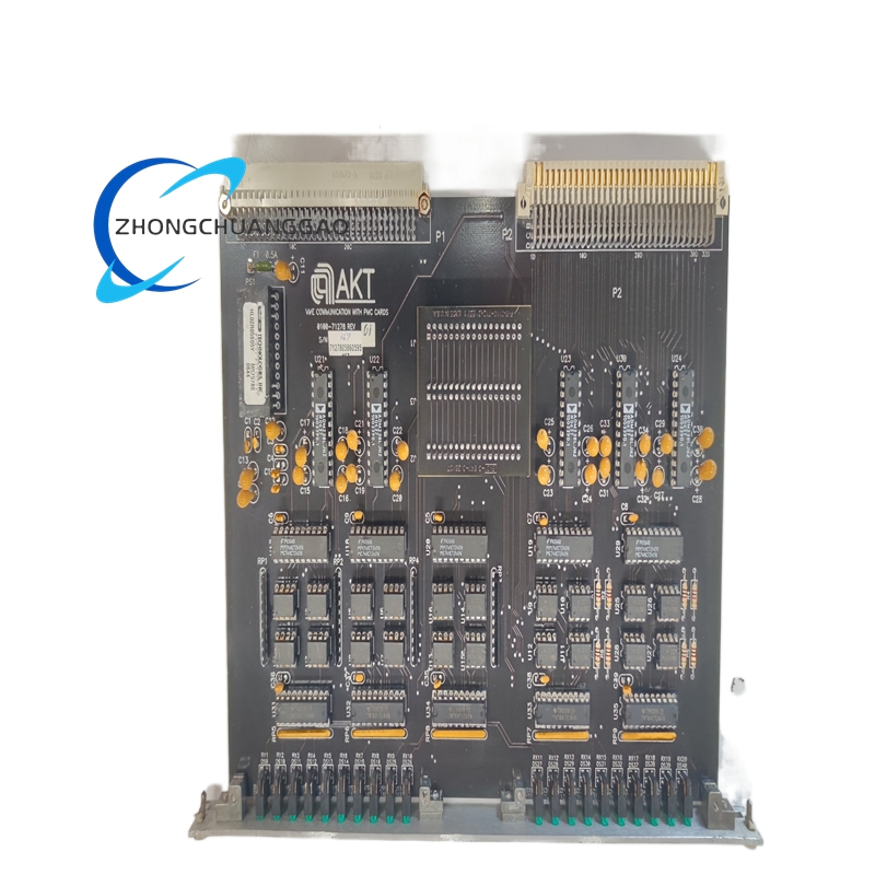
AMAT Semiconductor Wafer Handling Component 0100-71278
Product Brief
Specialized OEM mechanical part for wafer transfer and positioning systems on AMAT semiconductor equipment. It undertakes wafer supporting, positioning and auxiliary handling tasks in automated wafer production lines.
Description
Technical Specifications
- Part Type: Wafer Support & Positioning Fixture
- Applicable Wafer Size: Standard semiconductor wafer dimension
- Operating Environment: High vacuum + plasma atmosphere
- Operating Temperature: Room temperature to 200 °C
- Positioning Accuracy: Micron-level positioning precision
- Cleanliness Class: Class 100 ultra-clean standard
Functional Features
- Provides stable mechanical support for wafers during processing
- Realizes precise wafer positioning for alignment operations
- Anti-sticking design to avoid wafer surface damage
- Low outgassing performance for vacuum environment application
Performance Parameters
- Load Capacity: Rated load matching standard semiconductor wafer weight
- Position Repeatability: Stable repeated positioning accuracy for mass production
- Outgassing Rate: Meets semiconductor vacuum system low outgassing requirements
- Vibration Resistance: Maintains stability under equipment cyclic movement
Material Composition
- Main Body: High-performance ceramic composite material
- Contact Surface: Ultra-smooth non-stick ceramic coating
- Reinforcement Structure: High-strength lightweight alloy framework
Structural Characteristics
- Multi-point contact support structure to reduce wafer contact area
- Symmetrical layout for uniform force bearing
- Integrated positioning bosses for precise alignment
- Curved surface design adapting to wafer outer contour
Working Principle
When wafers enter the process station, this component contacts and supports the wafer from the bottom and side positions. It fixes the wafer at the designated processing position, ensures no displacement during process reaction, and cooperates with robotic arms to complete automatic wafer loading and unloading.
Advantage Highlights
- Ceramic material features ultra-low particle generation and low outgassing
- Minimal contact area effectively protects wafer surface integrity
- Excellent high-temperature stability with no thermal deformation
- Fully compatible with AMAT automated wafer handling systems
Applicable Industries
Semiconductor wafer fabrication, chip packaging process, microelectronics manufacturing, solar cell wafer production
Installation Requirements
- Assemble inside Class 100 ultra-clean workshop with anti-static gloves
- Calibrate horizontal level and positioning accuracy after installation
- Ensure no sharp edges on contact surfaces that may scratch wafers
- Fix all mounting parts firmly to eliminate operational vibration
Usage Notes
- Inspect contact surfaces for foreign particles before equipment startup
- Avoid impact and collision during equipment maintenance
- Replace immediately if surface wear or chipping is found
- Do not use in environments beyond rated temperature range

Reviews
There are no reviews yet.