
Product Short Description
Product Overview
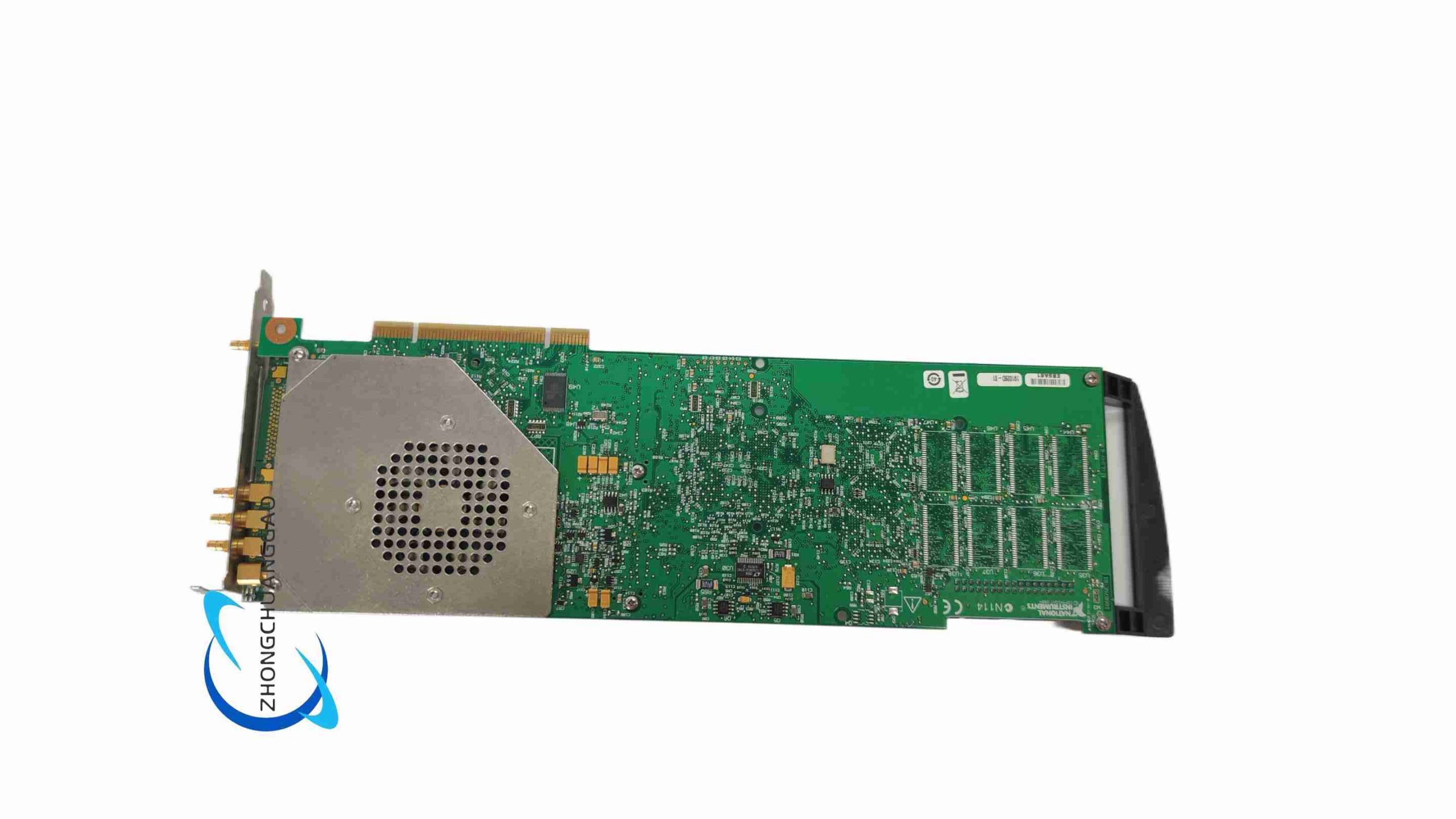
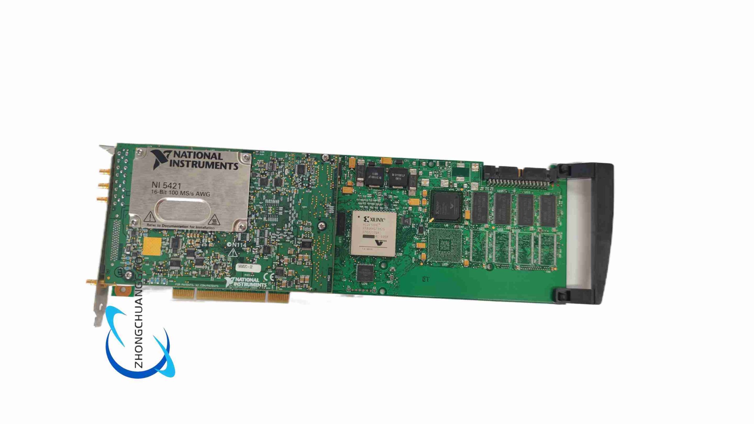
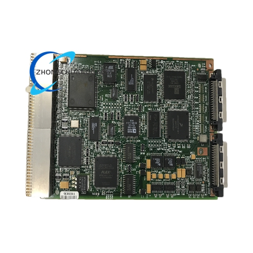
The PCI-5421 is a high-speed PCI-bus arbitrary waveform generator (AWG) designed for electronic test, RF component characterization and mixed-signal stimulus generation. It delivers single-channel high-bandwidth analog output with 100 MS/s maximum sampling rate, supporting standard periodic waveforms and fully user-defined arbitrary waveform generation with large onboard waveform memoryNI
Description
Analog Output Channel
- Channel Count: 1 single-ended analog output channel
- DAC Resolution: 16-bit digital-to-analog converter
- Maximum Sampling/Update Rate: 100 MS/s
- Supported Waveform Types: Standard sine, square, triangle, ramp-up/ramp-down; fully custom arbitrary user-defined waveforms
Output Voltage & Impedance Parameters
- Peak-to-Peak Output Voltage: 12 Vpp into 50 Ω load
- DC Offset Range: ±25% of full peak-to-peak output amplitude
- Software-Selectable Output Impedance: 50 Ω or 75 Ω matching for RF and communications test fixtures
- Programmable Attenuation Range: 0 dB to 51 dB adjustable attenuation
Frequency Generation Limits
- Maximum Sine Wave Frequency: 43 MHz
- Maximum Square Wave Frequency: 12.5 MHz
- Maximum Triangle/Ramp Wave Frequency: 5 MHz
Clock & Timing Subsystem
- Three Independent Sample Clock Modes:
- Divide-by-N Internal Clock: RMS jitter < 1.0 ps, phase noise -137 dBc/Hz at 10 MHz carrier, 10 kHz offset
- DDS High-Resolution Internal Clock: Sampling rate resolution 1.06 µHz for ultra-fine frequency tuning
- External Clock Input via SMB front panel connector
- Synchronization Interfaces: RTSI bus multi-board phase locking; NI-TClk timing synchronization protocol; PLL lock to external 10 MHz reference clock
Onboard Waveform Memory
- Maximum Onboard Storage Capacity: 256 MB dedicated waveform memory
- Memory Operation Functions: Waveform looping, multi-segment waveform linking, real-time streaming waveform data transfer from host PC RAM
Trigger & Marker I/O
- External Trigger Input Count: 4 independent TTL trigger input lines
- Marker Event Outputs: 4 programmable digital marker trigger outputs for external test equipment synchronization
- Optional Digital Pattern Generation: 16-bit LVDS digital pattern output with synchronized sample clock
3.4 Functional Features
- 100 MS/s high-speed arbitrary waveform generation for RF, communications and semiconductor component testing
- DDS high-resolution clock architecture offering microhertz-level frequency adjustment precision
- Large 256 MB onboard waveform memory supporting long-duration looping and multi-segment linked arbitrary waveforms
- Software-selectable 50/75 Ω output impedance matching for RF test fixtures and coaxial cable impedance matching
- Multi-stage programmable attenuation (0–51 dB) to adjust output signal amplitude for low-level component characterization
- Integrated digital marker outputs synchronized with analog waveform generation to trigger oscilloscopes, spectrum analyzers and external data acquisition hardware
- NI-TClk and RTSI bus synchronization enabling multi-AWG phase-locked multi-channel stimulus generation systems
- Full NI-DAQmx driver compatibility with LabVIEW, MATLAB, Python, C/C++ and Visual Studio development environments
- Built-in digital and analog low-pass anti-imaging filters to suppress high-frequency spurious output harmonics
3.5 Application Scenarios
- RF transceiver, filter and power amplifier component characterization testing
- Communications protocol signal generation for cellular, radar and sonar system simulation
- Semiconductor mixed-signal IC production test and validation
- Automotive electronic control unit (ECU) sensor signal emulation
- Audio amplifier and speaker frequency response stimulus testing
- Ultrasonic transducer excitation signal generation for non-destructive material inspection
- High-speed digital circuit clock and timing signal emulation
3.6 Performance Parameters (Typical at 25°C)
- Operating Temperature Range: 0 °C to 55 °C
- Storage Temperature Range: -40 °C to 85 °C
- Total Peak Power Consumption: 21.9 W
- Minimum External Clock Input Duty Cycle Tolerance: 40% to 60%
- Output Short-Circuit Protection: Indefinite short-circuit tolerance with automatic current limiting
3.7 Material & Construction Composition
- Main Printed Circuit Board: Multi-layer FR-4 high-frequency low-loss circuit board with dedicated analog, digital and power ground plane separation to minimize RF signal attenuation and crosstalk
- Core Processing Hardware: High-speed 16-bit DAC chip, Xilinx high-performance FPGA waveform memory controller and timing generator, DDS frequency synthesis IC
- Front Panel Connectors: SMB coaxial RF connector for analog waveform output; multi-pin D-SUB connector for digital trigger, marker and LVDS pattern signals
- Mechanical Mounting Hardware: Zinc-plated cold-rolled steel full-height PCI retention bracket
- Passive RF Components: Low-loss ceramic RF capacitors, precision thin-film resistors, ferrite EMI suppression beads, high-frequency coaxial signal traces with controlled impedance matching
3.8 Structural Characteristics
- Form Factor: Standard full-length 32-bit PCI 33 MHz bus compliant expansion board
- Physical Dimensions: 10.6 cm width × 17.5 cm length
- PCB Layout Isolation: Strict physical separation of high-frequency RF analog output circuitry and digital FPGA/PCI bus logic via full copper ground guard rings to eliminate digital switching noise coupling to RF signal paths
- High-Frequency Controlled Impedance Traces: All analog RF signal PCB traces manufactured to precise 50 Ω characteristic impedance specifications to prevent signal reflection and attenuation
- Thermal Dissipation Design: Dense copper thermal vias under high-power FPGA and DAC chips for passive convection heat dissipation; surface-mount thermal pads for heat transfer to chassis mounting bracket
- EMI/RF Shielding: Continuous copper ground shielding layer surrounding all RF analog signal traces to block external electromagnetic interference and prevent internal RF signal leakage
3.9 Working Principle
- Waveform Data Storage & Management: User-defined arbitrary waveform data or standard waveform mathematical parameters are transmitted from host PC to PCI-5421’s 256 MB onboard waveform memory via PCI bus high-speed DMA data transfer; FPGA memory controller supports multi-segment waveform linking and infinite waveform looping without continuous host PC data streaming
- High-Precision Clock Generation: Onboard clock subsystem generates sample clock signals via three selectable modes; DDS high-resolution clock synthesizer creates ultra-fine adjustable frequency reference with 1.06 µHz tuning resolution; Divide-by-N clock delivers ultra-low jitter for high-frequency RF signal generation
- Digital Waveform Synthesis: FPGA timing controller reads stored waveform sample data from onboard memory at the precise sample clock rate; digital gain and attenuation stages adjust sample amplitude values according to user-defined attenuation settings; digital low-pass anti-imaging filters suppress high-frequency image harmonics generated during digital-to-analog conversion
- 16-Bit Digital-to-Analog RF Conversion: Filtered digital waveform samples are fed to high-speed 16-bit DAC chip; DAC converts discrete digital sample values to continuous analog RF voltage signal; output impedance matching circuit configures signal path for 50 Ω or 75 Ω load impedance matching
- Trigger & Marker Synchronization Logic: Onboard FPGA continuously monitors external TTL trigger input lines; upon detection of valid trigger edge, waveform generation sequence initiates synchronously; programmable digital marker signals are output at user-defined waveform sample positions to synchronize external test and measurement instruments
- Multi-Board Phase-Locked Synchronization: RTSI bus and NI-TClk timing protocols share master clock and trigger signals across multiple PCI-5421 boards, enabling fully phase-aligned multi-channel arbitrary waveform stimulus generation systems for complex multi-signal test setups
3.10 Installation Requirements
- Host PC Expansion Slot: Unoccupied full-length 32-bit PCI motherboard expansion slot; host PC chassis must support active forced-air cooling to maintain rated 0–55 °C operating temperature range
- Mechanical Installation Procedure: Remove chassis metal slot blank plate; align PCI board gold edge connector with motherboard PCI slot; fully insert edge connector until fully seated; tighten steel retention bracket screw firmly to chassis frame to eliminate PCB mechanical vibration
- RF Coaxial Wiring Specifications: Use 50 Ω or 75 Ω low-loss RF coaxial cable matching board output impedance setting for all analog waveform output connections; minimize coaxial cable length to reduce RF signal attenuation; secure coaxial cable SMB connectors tightly to prevent signal reflection and intermittent connection noise
- Digital Trigger Wiring Rules: Use shielded twisted-pair cable for all digital trigger and marker signal wiring; separate digital control cables from RF analog coaxial cables by minimum 20 cm physical distance to avoid electromagnetic interference-induced signal distortion
- Software Driver Installation: Install latest NI-DAQmx driver suite compatible with Windows/Linux host operating system; launch NI MAX hardware configuration utility to automatically detect PCI-5421 hardware and verify clock, memory and output channel functionality
3.11 Operation Precautions
- RF Output Overload Protection Limit: Do not connect analog output channel to DC voltage sources exceeding ±12 V peak; external DC voltage overload will permanently damage high-speed DAC output circuitry
- ESD Static Discharge Safety Protocol: Mandatory grounded anti-static wristband usage before physical contact with PCB, SMB RF connectors or internal circuit components; electrostatic discharge irreparably damages high-frequency RF DAC and FPGA chips
- Chassis Cooling Mandate: Never operate PCI-5421 with host PC chassis side panel removed; insufficient convection airflow causes severe thermal drift, increased output signal noise and degraded RF signal spectral purity
- Coaxial Cable Impedance Matching Rule: Always use coaxial cable with impedance matching the board’s software-selected output impedance (50 Ω / 75 Ω); mismatched cable impedance causes RF signal reflection, amplitude attenuation and waveform distortion
- Calibration Maintenance Schedule: Execute onboard signal calibration every 30 days of continuous operation; complete full external factory calibration with NI certified RF reference signal equipment once per calendar year
- Storage Environment Requirements: When uninstalled from host PC, store PCI-5421 in original factory anti-static RF shielding packaging; avoid long-term storage in high-humidity, dusty or extreme temperature environments
- External Clock Input Voltage Limit: Do not apply external reference clock input voltage exceeding 3.3 V TTL logic level; excessive input voltage will damage front-end clock receiver circuitry
Reviews
There are no reviews yet.