
Product Short Description
Product Overview
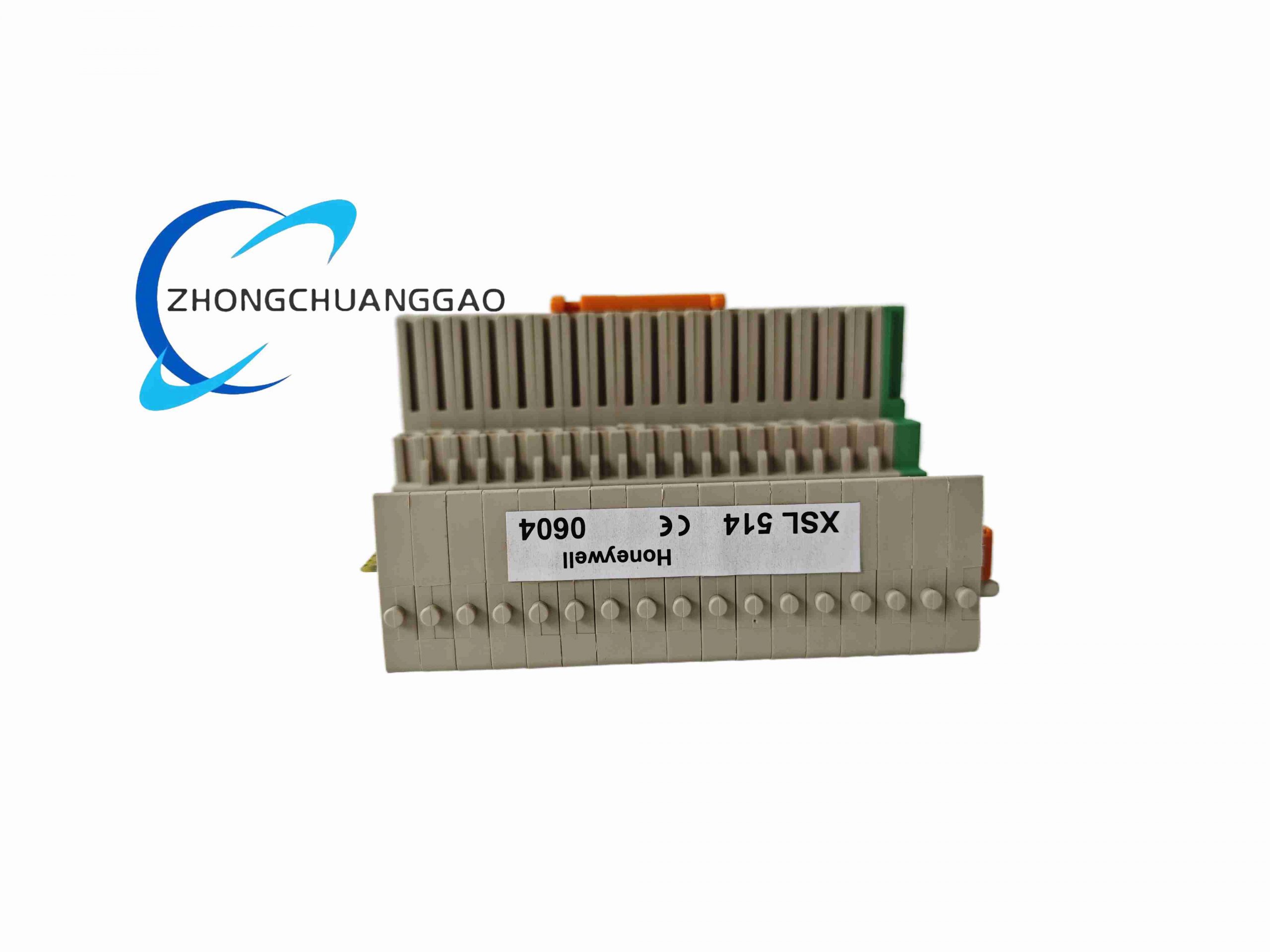
High-speed industrial vision signal processing module developed by Matrox for automated machine vision inspection equipment, receiving multi-channel industrial camera digital image signals and completing pre-processing operations such as image filtering, feature extraction and signal buffering before transmitting data to industrial host computers for defect detection algorithms. Widely used in precision manufacturing visual inspection production lines.
Description
Technical Specifications
- Camera Input Channels: 4 independent LVDS Camera Link base configuration input ports
- Supported Camera Modes: Area-scan cameras, single-channel line-scan cameras, monochrome & color Bayer pattern sensors
- Total Aggregate Bandwidth: Maximum 1.2 Gbps cumulative input bandwidth across four active channels
- Onboard Processing Hardware: Integrated industrial-grade FPGA with dedicated vision acceleration logic
- Image Buffer Memory: 2 GB high-speed DDR4 onboard frame memory for multi-frame storage without host dependency
- Host Interface: PCI Express 2.0 x4 edge connector, full-duplex bidirectional data transmission
- Pixel Bit Depth Support: 8-bit, 10-bit, 12-bit, 14-bit raw pixel input conversion
- Trigger Signal I/O: 8 isolated digital trigger inputs, 4 strobe pulse outputs for synchronized camera lighting control
- Power Input: 12 V DC internal industrial PC power rail, maximum power draw 28 W
- Physical Form Factor: Standard half-length low-profile PCIe add-in card, dimensions 168 mm (L) × 111 mm (H) × 21 mm (D)
- Net Weight: 0.42 kg
- Operating Environmental Parameters: Operating temperature range 0 °C ~ +60 °C inside industrial PC chassis; storage temperature -40 °C ~ +85 °C; relative humidity 5%–90% non-condensing
- EMC Compliance: CE Class A industrial electromagnetic compatibility certification
- Software Compatibility: Matrox Imaging Library (MIL), MIL-Lite, Windows 10/11 IPC, Linux Ubuntu industrial kernel
Core Functional Features
- Simultaneous synchronous capture from four LVDS cameras with microsecond-level trigger synchronization accuracy
- Hardware-accelerated preprocessing functions including median noise filtering, flat-field correction, dark pixel subtraction, color demosaicing and contrast stretching
- Large 2 GB onboard frame buffer enables continuous image caching during temporary host communication bottlenecks to avoid frame loss
- Isolated digital trigger and strobe output terminals coordinate camera exposure timing with LED machine vision lighting systems
- Independent channel configuration; each camera port supports unique resolution, exposure and pixel bit depth settings without cross-channel interference
- Built-in signal integrity diagnostics for LVDS cables, automatically reporting cable attenuation, pin short circuits and camera disconnection faults to host software
- Low-profile half-length design compatible with compact fanless industrial box PCs and rack-mounted vision workstations
- FPGA firmware upgradable via software without hardware replacement to add new camera protocol support
Working Principle
LVDS serialized image data streams from each connected industrial camera enter dedicated differential signal receivers on the XSL514 PCB. Signal integrity circuits eliminate high-frequency factory noise induced by servo motors and inverters before pixel data is forwarded to the onboard FPGA accelerator chip. The FPGA executes user-defined preprocessing algorithms in parallel across all four channels; processed pixel frames are temporarily stored in the 2 GB DDR4 buffer memory. When the host industrial PC requests image data, the PCIe x4 interface transmits buffered frames to system RAM in burst transfer mode to maximize throughput. External trigger signals synchronize camera exposure with production line encoder pulses, while strobe outputs fire inspection lighting to freeze moving target imagery. Continuous real-time channel monitoring compares incoming LVDS signal levels against calibrated thresholds to flag faulty wiring or disconnected cameras instantly.
Structural & Material Characteristics
- Main Circuit Substrate: Multi-layer high TG FR4 PCB with full ground plane shielding to suppress electromagnetic crosstalk between LVDS signal traces and PCIe power circuits
- External Heat Dissipation: Extruded black aluminum passive heat sink bonded directly to FPGA and memory chips, eliminating the need for noisy cooling fans
- Signal Connectors: Gold-plated MDR 26-pin Camera Link LVDS ports with locking screw fasteners to prevent loose cable connection under production line vibration
- Trigger Terminal Block: Screw-type industrial terminal headers with galvanic optocoupler isolation between external 24 V trigger signals and onboard logic circuits
- Card Bracket: Cold-rolled steel anti-vibration PCIe mounting bracket with grounding lug for cabinet ESD protection
- Internal Component Packaging: Industrial temperature-grade FPGA, DDR4 memory and differential signal receivers rated for continuous 60 °C operation
Installation Requirements
- Insert into a vacant PCIe Gen2 x4 or higher expansion slot inside an industrial vision PC; avoid sharing slots with high-power GPU cards that generate excess heat
- Secure the metal mounting bracket to the PC chassis grounding rail to complete full EMC shielding and static discharge path
- Maintain minimum 30 mm vertical airflow clearance above the aluminum heat sink; blocked ventilation causes thermal throttling of FPGA processing speed
- Use only shielded twisted-pair Camera Link LVDS cables with metal shielding shell single-point grounded at the card bracket end
- Route trigger/strobe wiring separately from high-current servo drive power cables with a minimum 40 mm separation gap to block induced electrical noise
- For fanless embedded IPC installations, install auxiliary chassis cooling fans to keep internal ambient temperature below 55 °C during continuous 24-hour operation
Application Scenarios
Electronic semiconductor wafer surface defect inspection, SMT printed circuit board solder joint quality testing, automotive component dimensional measurement, pharmaceutical blister package visual defect detection, lithium battery electrode surface inspection, food packaging label print verification, precision metal part surface scratch detection, high-speed web printing defect monitoring.
Operation & Maintenance Precautions
- Mandatory ESD wristband grounding when handling or installing the PCIe card; ungrounded static discharge permanently damages sensitive LVDS differential receiver chips
- Do not hot-swap LVDS camera cables while the module and industrial PC remain powered; live cable disconnection creates voltage surges that burn channel input circuits
- Clean the aluminum heat sink surface every 3 months in dusty factory environments to remove accumulated dust blocking passive heat dissipation
- Perform cable signal integrity testing monthly via Matrox MIL diagnostic tools to identify gradual LVDS cable attenuation before image distortion occurs
- Complete firmware upgrades only during scheduled production downtime; live firmware flashing interrupts all camera image capture operations
- Avoid mounting the host PC near high-frequency inverters or large contactors; strong electromagnetic interference triggers frame corruption and trigger signal misalignment
- Do not connect 24 V AC voltage to digital trigger input terminals; overvoltage destroys optocoupler isolation components instantly
Reviews
There are no reviews yet.