Product Short Description
- Product Name: 2114B-30SLT Semiconductor Inspection & Metrology Component
- Product Introduction: High-precision optical detection component for semiconductor wafer, chip and microelectronic product surface defect inspection and dimension measurement.
- Technical Specifications:
- Optical Detection Resolution: Sub-micron level
Description
-
- Operating Environment: Class 100/Class 1000 clean room standard
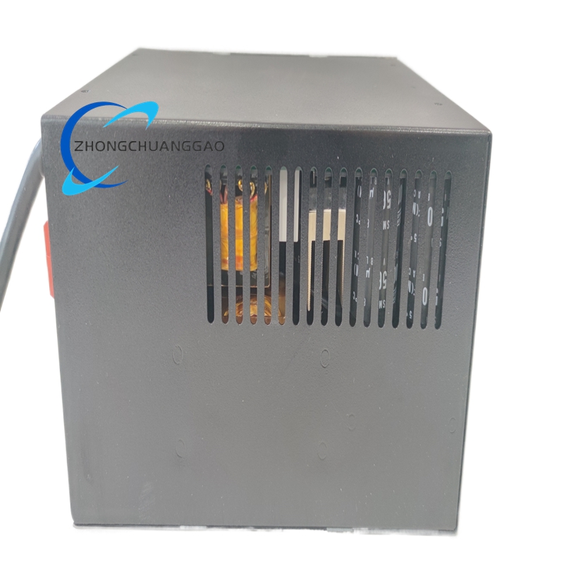
- Operating Voltage: 100 ~ 240 V AC, 50/60 Hz
- Working Humidity: 40% ~ 60% RH, non-condensing
- Detection Range: Full coverage of semiconductor wafer surface
- Functional Features: Surface defect scanning, particle detection, pattern inspection, micro dimension measurement; High-speed automatic scanning; Image acquisition and data output.
- Performance Parameters: Scanning Speed: High-speed continuous scanning; Detection accuracy up to 0.1 μm; Stable operation for 24/7 continuous work.
- Material Composition: High-purity aluminum alloy structural parts; High-transmittance optical glass; Precision optical lens group; Dust-proof sealing rubber parts.
- Structural Characteristics: Precision integrated optical structure; Fully sealed dust-proof design; Modular optical path assembly; Vibration damping base structure.
- Working Principle: Emit high-precision optical beam to irradiate the surface of semiconductor products, collect reflected and scattered light signals through optical sensors, analyze signal changes to judge surface defects, scratches, particles and dimensional deviation.
- Advantages & Highlights: Ultra-high detection precision; Strict dust-proof and anti-pollution performance; Stable optical path; Meet semiconductor manufacturing high-standard requirements.
- Applicable Industries: Semiconductor manufacturing, wafer processing, chip packaging, microelectronics, precision photoelectric industry.
- Model Series: KLA-Tencor 2114B Optical Inspection Series
- Installation Requirements: Install in professional clean room; Equip with vibration isolation base; Strictly control ambient dust and humidity; Fix optical components without displacement.
- Usage Notes: Prohibit contact with optical lens surface; Strictly follow clean room operation specifications; Regularly perform optical path calibration; Avoid impact and vibration.
Reviews
There are no reviews yet.