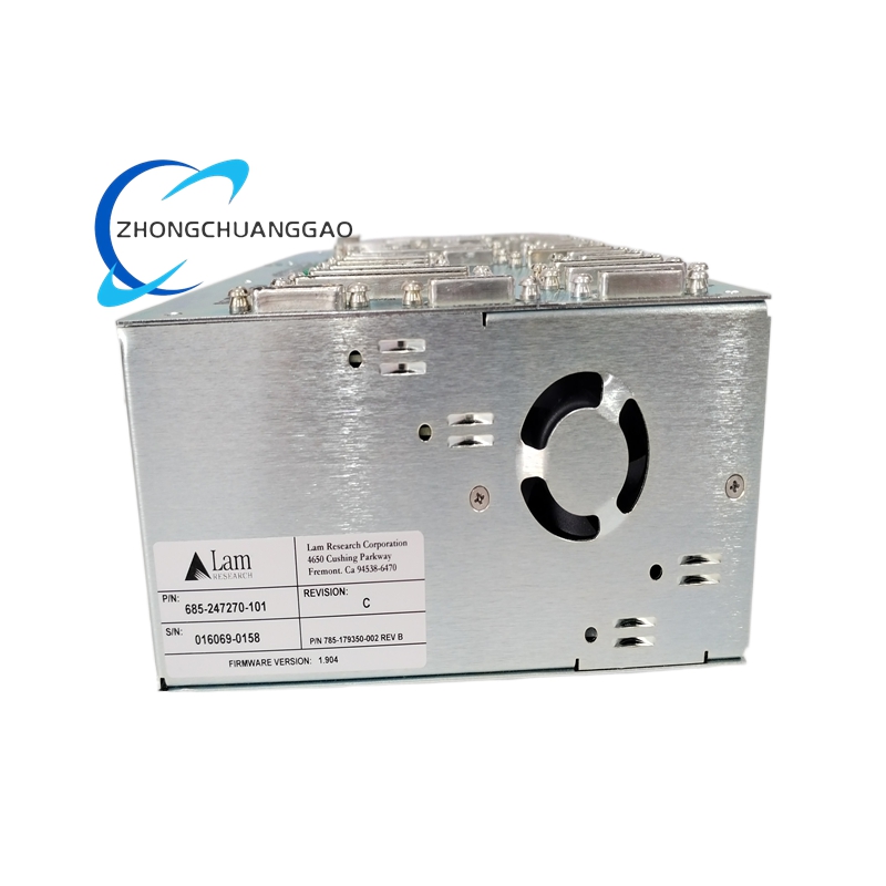
Product Short Description
- Product Name: Semiconductor Plasma Chamber Component
- Brief Introduction: Core structural part of LAM plasma etching chamber, bearing plasma reaction and mechanical sealing functions.
- Technical Specifications: Plasma working power matching 13.56 MHz RF power, working vacuum 8×10⁻⁸ Torr, maximum withstand temperature 150 °C, sealing width 12 mm.
Description
- Functional Features: Forms closed plasma reaction cavity, isolates external environment, bears plasma radiation and process gas erosion.
- Performance Parameters: Gas leakage rate ≤ 5×10⁻¹⁰ sccm/sec, continuous working time ≥ 48,000 hours, plasma radiation resistance grade Level A.
- Material Composition: High-purity ceramic main body + special anti-plasma coating + elastic metal sealing assembly.
- Structural Characteristics: Circular integral structure, multi-layer composite sealing design, embedded positioning groove, symmetrical stress structure.
- Working Principle: Creates closed space required for plasma chemical reaction under high vacuum, isolates process gas and plasma, and maintains stable internal environment of reaction chamber.
- Advantages: Excellent plasma erosion resistance, ultra-low air leakage, uniform stress distribution, long service cycle.
- Applicable Industries: Semiconductor chip manufacturing, plasma etching, microelectronics processing, advanced packaging process.
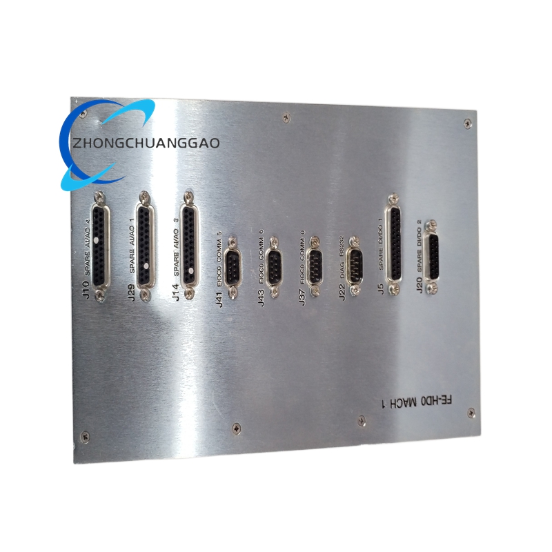
- Series Information: LAM 685 Series Plasma Chamber Core Components, 101 is the first-version configuration.
- Installation Requirements: Complete installation in Class 10 ultra-clean workshop; use special fixture for positioning; apply designated sealing auxiliary materials.
- Usage Precautions: Prohibit mechanical scratching on coating surface; stop equipment before disassembly; inspect sealing surface integrity during routine maintenance.
Reviews
There are no reviews yet.